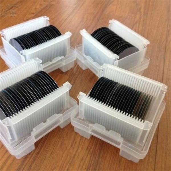
Single Crystal Monocrystalline Silicon Wafer
Monocrystalline silicon wafer refers to the silicon material grown from a single crystal, which has a high degree of purity and uniformity. In semiconductor manufacturing, single crystal silicon wafers are one of the important materials for making integrated circuits, solar panels and other electronic components.
Deskrizzjoni
Products Description
Monocrystalline silicon wafers are the basic materials for the manufacture of various semiconductor devices, such as integrated circuits, transistors, diodes, etc. These devices are a core component of modern electronic devices, and the purity and crystal structure of single-crystal silicon wafers have a critical impact on device performance.
Monocrystalline silicon wafers have the advantages of good high-temperature stability and strong oxidation resistance, so they are also used in the field of high-temperature heat treatment. For example, single crystal silicon wafers can be used to manufacture high-temperature equipment such as quartz glass processing tools and optical instruments.
Specification
| Name | Silicon wafer |
| Type | P or N |
| Orientation | <100>or<111> |
| Diameter | 2-8 inch |
| Tolerance | ±5mm |
| Thickness | 180-2000μm |
| Tolerance | ±10μm |
| Dislocation Density(pcs/Cm2) | None |
| Resistivity | 0.001-10000 Ω.cm |
| Purity | 6N-9N |


FAQ
Q:what are your main products?
A:Single Crystal Silicon (Optical silicon wafer,silicon ball,Etching silicon wafer.Silicon oxide wafer)
Q: Are you trading company or manufacturer ?
A: We are factory.
Q: How long is your delivery time?
A: Generally it is 5-10 days if the goods are in stock. or it is 15-20 days if the goods are not in stock, it is according to
quantity.
Q: Do you provide samples ? is it free or extra ?
A: Yes, we could offer the sample for free charge but do not pay the cost of freight.
It-tags Popolari: single crystal monocrystalline silicon wafer
Ibgħat l-inkjesta
Tista 'Tħobb ukoll


